

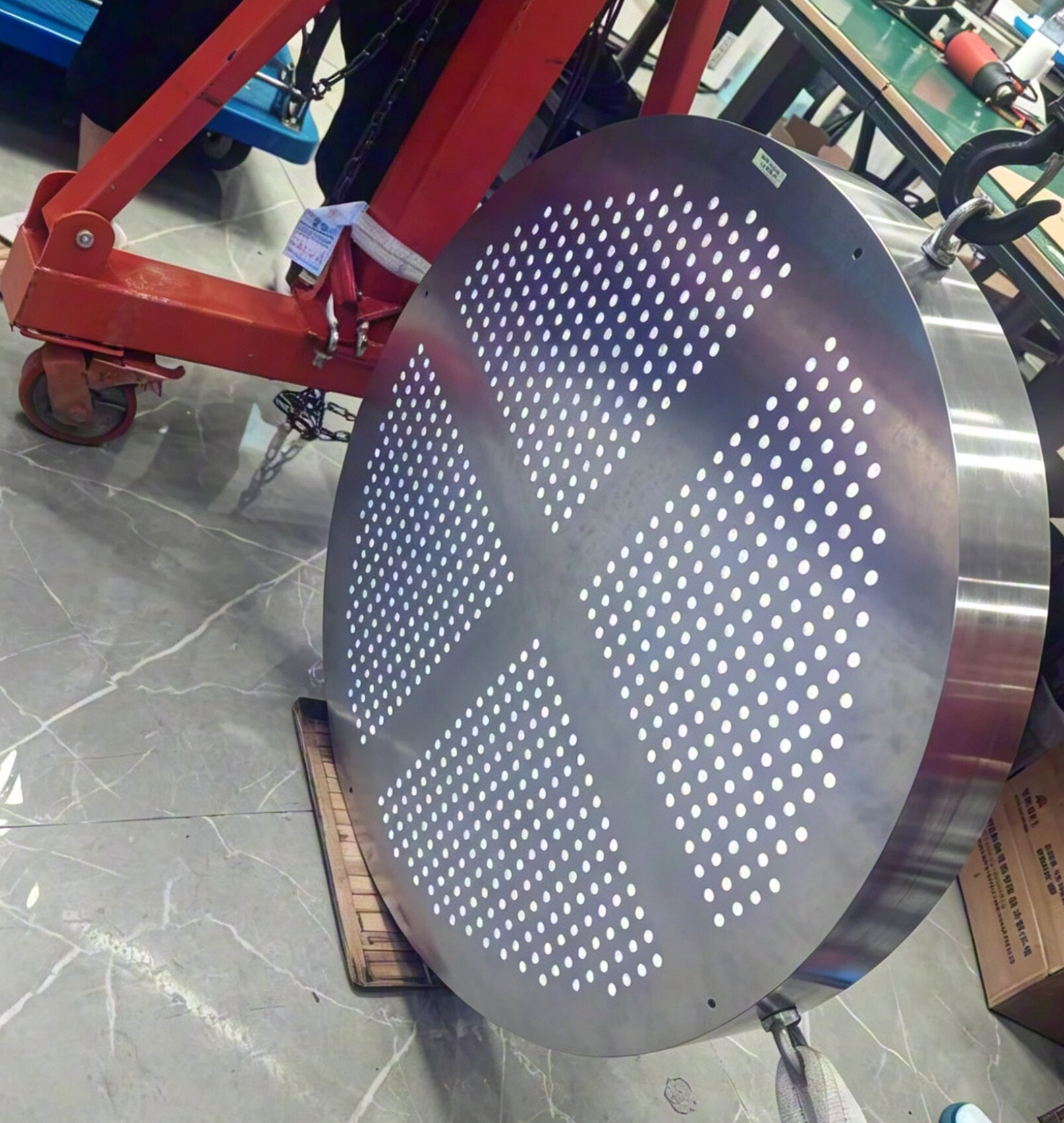
Worlds First 1m Diameter 3000W UV LED Disc for SiC Substrate Surface Modification
Posted by LEDINTRO | Industrial High-Power UV LED Manufacturer
Groundbreaking R&D Achievement
After two months of dedicated R&D breakthroughs, LEDINTRO has independently developed the world’s first 1-meter diameter UV LED disc module, specially customized for surface modification processes of 4th-generation semiconductor silicon carbide (SiC) substrates.
This innovative large-area UV light source fills the market gap of integrated whole-wafer UV activation treatment, bringing stable, ultra-high intensity uniform irradiation to mass SiC wafer production lines.
Core Technical Specifications
- Total Output Power: 3000W
- Full-surface Light Uniformity: 90%
- Peak Irradiance: Over 500mW/cm²
- Irradiation Format: Complete circular 1m diameter uniform exposure area
Key Product Advantages for SiC Wafer Processing
-
Full-size circular irradiation surfaceThe 1-meter integral disc matches large-size SiC wafer batch processing, realizing one-time full-piece UV treatment without segmented splicing.
-
Ultra-consistent UV output across entire substrate90% high uniformity eliminates local difference in surface modification effect, ensuring stable wafer quality and boosting production yield.
-
High irradiance for higher throughputUp to 500mW/cm² high irradiation intensity shortens substrate activation time, significantly lifting the production capacity of wide-bandgap semiconductor factories.
Why Traditional Linear UV Sources Fall Short
Conventional segmented linear UV lamp arrays cannot deliver synchronized, uniform irradiation over a complete large SiC wafer. Separate splicing irradiation leads to inconsistent modification results and extra production handling steps.
Our all-in-one circular UV LED disc solves this pain point perfectly, directly upgrading the efficiency and stability of next-gen wide-bandgap semiconductor mass-production lines.
LEDINTRO Custom UV LED Solutions
We specialize in customized high-power industrial UV LED modules for semiconductor, electronics curing and advanced material processing.
Our engineering team provides full support including:
- Custom power & size UV light source development
- Datasheets & performance test reports
- Free sample testing service
- OEM & ODM module cooperation
If you are engaged in SiC wafer manufacturing, wide bandgap semiconductor R&D or semiconductor equipment integration, contact our technical team to get detailed parameters and customized solution consultation.